
A year before the first iPhone launched (2007), I worked on improving the robustness of WiFi chipsets for mobile devices using a data modulation technique called Orthogonal Frequency Division Multiplexing (OFDM). My main focus was developing a low power design for an OFDM core, which would minimize battery drain; thus avoiding the need for bigger batteries which raise the cost of a mobile device. I did this work under the guidance of Professor Vijay Madisetti with Mohanned Sinnokrot as my graduate mentor, during the Spring 2006 semester at Georgia Tech. Although we did not publish, I made the code open source in 2007. It appears that atleast one research paper using my code (and apparently my figures too) was published in 2014.
1. Problem Statement
1.1 Radios on Mobile Devices:
The number of radios (e.g. GSM/CDMA, WiFi, Bluetooth, GPS) present on mobile devices are expected to grow in the service of enabling rich integrated mobile user experiences. On mobile devices, these radio chipsets account for roughly a third of the power consumption. More radios mean higher power consumption and more frequent charging of batteries which limits how ‘mobile’ a mobile device really is. Increases in battery capacity and size offer one solution to this problem, but this approach is limited by how big (and expensive) a commercially successful mobile device can be. Low power designs tailored for mobile devices are an important engineering approach to improve battery life and keep costs low for consumers.
1.2 The case of WiFi radios:
WiFi radios are a near certain presence on mobile devices, enabling better connectivity and greater bandwidth for endusers. Compared to WiFi on Desktops/Laptops, Mobile WiFi is subject to more diverse and challenging conditions, like overloaded Wireless Access Points (e.g. Starbucks at Tech Square) or locations with poor signal strength on a college campus (e.g. the Campanile on Tech campus). These conditions can lead to higher error rates which translate to slower WiFi.
1.3 Making Mobile WiFi Robust:
In order to tackle challenging conditions that arise in Mobile WiFi, the 802.11 WiFi standard includes the option to implement Orthogonal Frequency Division Multiplexing (OFDM) [1]. OFDM is a data modulation technique that can cope with severe conditions on the wireless ‘channel’ while maintaining low error rates. OFDM partitions the frequency band into smaller, overlapping but orthogonal sub-carrier bands. Data is transmitted in parallel over these sub-carrier bands, resulting in better error resilience in the face of issues like inter-symbol interference (ISI) and multi-path fading. There is much to learn about how and why OFDM works [2] (we will not do that here) and it can be used in wireless communications in standards outside of WiFi too.
1.4 Great, let us do OFDM!
Here is a simplified block diagram for an OFDM engine. The red and green indicate the data flow and computation involved in the transmit and receive configurations respectively.
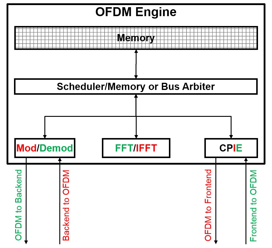
Data is modulated (or demodulated) before being put through a Inverse Fourier Transform (or a Fourier Transform) before Cyclic Prefixing (Insertion or Extraction), which is essentially adding/removing padding around the actual data trasmitted to (or received from) the WiFi radio. The modules do not hand off data directly to each other. Instead they read from/write to common memory, accessed through a shared bus.
There is a lot going on here and we will not get into all the details. However, I will note that the Fourier Transform (and Inverse Fourier Transform) is the computationally expensive (and therefore power hungry) part of this whole process. This project focused on making that block of the OFDM engine more efficient.
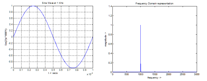
At the heart of OFDM is the Discrete Fourier Transform (DFT). Discrete Fourier Transforms convert signals from the time domain to the frequency domain. As an example, in the figure below a sinusoidal wave at 1 KHz visualized over time (left) is transformed via a DFT into the frequency domain where it shows up as a spike at 1 KHz (right).
1.5 Not so Fast (Fourier Transforms):
Discrete Fourier Transforms are computationally intensive (i.e. they take a lot of mathematical operations which cost energy to execute in a digital circuit).
Let us make this statement more concrete. Consider a $N$ point sequence of data given by x[1],…,x[N], the DFT gives us a $N$ point sequence X[1],…,X[N] via the following calculation
\[X[k]=\displaystyle\sum_{n=1}^{N}x[n] e^{-j\times\frac{2\pi n}{N}k}~,~~\forall~k~\in~[1,N]\]It is easy to see that computing each of the $N$ $X[k]$’s requires approximately 2N computations each (specifically N multiplication and N-1 addition operations). Thus, computing $X[k]~\forall~k~\in~[1,N]$ requires $O(N^2)$ computations.
More computational operations consume more energy making a procedure with exponentially growing computational cost quite undesirable. Fortunately, there already exists a more efficient way to implement Fourier Transforms through the Fast Fourier Transform (FFT) Algorithm [3]. The FFT reduces computational cost from $O(N^2)$ (blue) to $O(N\log(N))$ (red) as visualized below. In practice, any hardware implementing Fourier Transform uses the FFT algorithm to do so.

2. Solution
2.1 Overview of Approach [Layperson Friendly]
The FFT algorithm, while efficient still requires lots of multiplications and additions. A digital multiplier takes more area to implement in silicon, relative to an adder. As a result of being a larger circuit, a multiplier also requires more power to operate. Can we implement the FFT for OFDM in WiFi 802.11 without a digital multiplier? The proposed design answers YES.
Next, the 802.11 WiFi standard requires a 64 point FFT, and it places a 3.2$\mu s$ timing constraint for the OFDM processing of a (64 point) symbol. Usually, one might be tempted to run the system at a faster clock (i.e. 40 MHz instead of 10 MHz). However, clocking a system faster increases the power consumption, so making the system efficient enough to perform a 64 point FFT in <3.2 $\mu$s at slow clock speeds is desirable for mobile WiFi chipsets implementing OFDM. Two possibilities (from many) to reduce clock speed were considered in this project.
First, can we identify where the engine spends time waiting and reduce (or eliminate) the delay at those bottlenecks? Memory access to read/write data is one such bottleneck. It usually takes more clock cycles to read/write data to/from memory, than it does to implement computation operations like addition/multiplication. This naturally begs the question, Can we reduce the number of memory accesses in an FFT processor? The proposed design answers YES, and cuts memory access (read/write) to 1/3rd of an unoptimized design.
Second, can we execute the algorithm to completion in fewer clock cycles, which would allow us to run the system at a slower clock and thus save power? The proposed design is single instruction single data (SISD) architecture, but it allows easy extension to a single instruction multiple data (SIMD) architecture that can reduce the number of clock cycles required to 1/8th. This would allow a corresponding reduction in clock speeds (and therefore reduce power consumption), while still meeting the 3.2 $\mu$s time constraint in the 802.11 standard.
Disclaimer: The two design considerations (clock speed, circuit size) mentioned here are the ones most relevant to this project. In general, low power digital design involves many more considerations that are not discussed here.
2.2 The FFT algorithm: complex butterfly and flow graphs
This section assumes that the reader is familiar with mathematical nuts and bolts of the FFT algorithm as described in Chapter 9 of Oppenheim and Schafer [4].
2.2.1 The complex butterfly computation
At the heart of the Cooley-Tukey Fast Fourier Transform Algorithm [3,4] is the complex butterfly calculation illustrated below.

Let us unpack this calculation a little bit.
- $A_{m-1},B_{m-1}$ are two complex numbers that serve as input. $A_{m},B_{m}$ are complex numbers representing the output.
- $m$ represents the ‘stage’ of the FFT algorithm being implemented by this algorithm
- $W$ represents the ‘twiddle factor’ involved with the given stage of the FFT.
- In full notation the twiddle factors are \(W^{k}_{N} = e^{\frac{2\pi jk}{N}}~,~~\forall~{k}~\in~[0,\frac{N}{2}-1]\).
- A $N=64$ point FFT has 32 twiddle factors ranging from $[W^{0}_{64},W^{31}_{64}]$, used in complex butterfly calculations at different stages of the FFT algorithm.
- We observe two additions and one multiplication (with $W$) of complex numbers in the butterfly. The division by two prevents arithmetic overflow and is a simple operation (no computational cost) in digital logic, because it involves shifting all the bits representing a number right once.
2.2.2 FFT Flow Graphs
Let us consider taking an FFT of an $N=8$ point signal to convert it from the time domain to the frequency domain. The flow graph below depicts all the complex butterfly operations in transforming time domain data into the frequency domain using the FFT algorithm. Note that the number of stages $M = 3 = log_2(8)$. Also observe that the in-place computation leads to a bit reversed index (i.e. 001 = 1 becomes 100 = 4) in the frequency domain which must be reordered before use in an application.

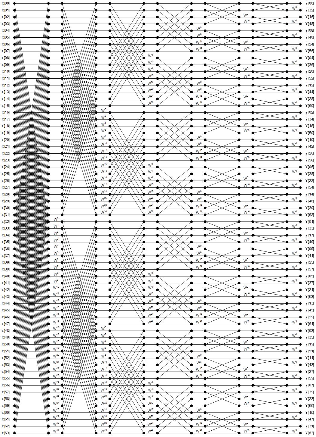
OFDM engines under the 802.11 standard rely on a $N=64$ point FFT/IFFT. The flow graph for a 64 point FFT is visualized below. It is denser and more extensive than the 8 point FFT flow graph above. It features $M = 6 = log_2(64)$ stages and 32 distinct twiddle factors.
2.3 Design
2.3.1 64 point FFT using Radix-8 flow graphs
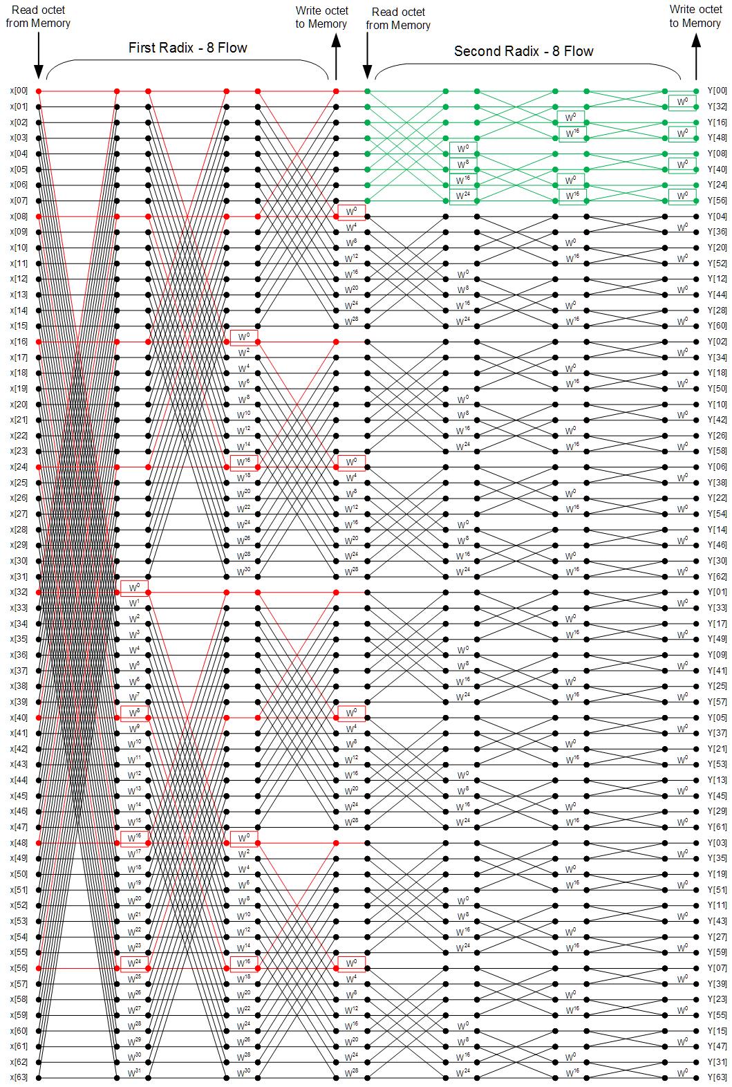
The design implements the 64 point FFT using radix-8 flow graphs as a building block. A single radix-8 flow completes 3 of the 6 butterfly computations for each term of the 64 point FFT. A radix-8 flow is executed on a an octet (8 terms) selected from the 64 point symbol. To complete the 64 point FFT, each of the input data are fed through radix-8 flows twice, each time as part of a different octet. Both the first and second radix-8 flows must be completed for each of the 64 input data points (i.e. 8 octets) in order to complete the 64 point FFT. The flow graph below visualizes the first octet for first radix-8 flow in red and the first octet for the second radix-8 flow in green. Memory reads and writes occur at the end of every radix-8 flow, with 2 read/write cycles occuring for each of the 64 inputs over the course of the FFT. This is a contrast to unoptimized designs, where a total of 6 memory read/write cycles at the beginning/end of each stage of the flow graph may slow down execution.
2.3.2 Architecture
The FFT processor has a modular design and comprises of three modules, the butterfly processor, the address generation unit (AGU) and the micro-coded state machine (MCSM). To perform an Inverse FFT, all we need to do is swap the real and imaginary parts.
The FFT data-path is visualized below without the AGU or MCSM. It depicts data flow from the point data enters the FFT processor module from memory, to the point where it is written back to memory. Red lines represent the control signals and their delayed versions. A ‘D’ is prefixed to represent the delayed versions of the original signal, each D signifies a single clock delay.

- The pipeline depicted above is 4 stages long and completes 3 stages of a radix-8 FFT calculation for an octet of the 64 point input data, before writing the data the data back to memory.
- The data is always read in from memory into Register Bank 1 and the data is always written out to memory from Register Bank 2.
- The two register banks allow 2 octets to be in the pipeline at any given time.
- The butterfly processor implements the complex butterfly discussed earlier and contains two pipelined stages.
- We avoid using a full digital multiplier to reduce footprint and reduce power consumption. Multiplication with different twiddle factors is realized using CSD (canonical signed digit multiplication, which uses shifters and adders to implement multiplication with known constants).
- The desired multiplication with any of the 32 twiddle can be obtained by passing the data through 2 CSD blocks which contain 8 and 4 unique constants respectively.
- The optimal number of shifters and adders for each block were identified by a code generation tool [5]
- Multiplexers control which combination of constants is used and together these blocks can replicate multiplication with any of the 32 unique twiddle factors in a 64 point FFT.
- All computations are done in place in memory. As a result they require a shuffle to address index bit reversal at the end.
- The 64 point FFT takes a total of 196 cycles.
The Address Generation Unit (AGU) which was not visualized above controls the address bus going to memory. The FFT processor reads and writes from and to the 8 dual port memory banks concurrently (each address is 3 bits). The address mapping scheme ensures that no memory location is read from and written to at the same time. There are 8 read address buses, and 8 write address buses. The computations are in place, which simplifies the address generation unit. The table below depicts the memory mapping scheme.
| Bank 0 | Bank 1 | Bank 2 | Bank 3 | Bank 4 | Bank 5 | Bank 6 | Bank 7 |
|---|---|---|---|---|---|---|---|
| 0 | 1 | 2 | 3 | 4 | 5 | 6 | 7 |
| 15 | 8 | 9 | 10 | 11 | 12 | 13 | 14 |
| 22 | 23 | 16 | 17 | 18 | 19 | 20 | 21 |
| 29 | 30 | 31 | 24 | 25 | 26 | 27 | 28 |
| 36 | 37 | 38 | 39 | 32 | 33 | 34 | 35 |
| 43 | 44 | 45 | 46 | 47 | 40 | 41 | 42 |
| 50 | 51 | 52 | 53 | 54 | 55 | 48 | 49 |
| 57 | 58 | 59 | 60 | 61 | 62 | 63 | 56 |
Finally, the Micro-Coded State Machine (MCSM) stores and generates all the control signals for the FFT processor’s operation at every one of the 196 cycles. Its progression is controlled by the clock. A reset signal en_fft resets the state machine counter and signals the beginning of a new 64-point FFT calculation. Upon completion the FFT processor asserts a done_fft signal to communicate the completion of the 64-point FFT. The number of states in the MCSM is 196.
3. Conclusion
The low power fft processor design proposed here for use in the OFDM engine of a 802.11 WiFi chipset implements a 64 point FFT without the use of a digital multiplier and minimizes idle time by using a radix-8 FFT as a building block that cuts memory access to 1/3rd of a conventional design. The design establishes a Single Instruction Single Data (SISD) that can be extended to Single Instruction Multiple Data (SIMD) in the future to run the processor at a slower clock and reduce power consumption while achieving the 3.2 $\mu$s time constraint set by the 802.11 standard. Other future opportunities for extension and improvement of this design include replacing the MCSM which generates the control signals with a compact logic based control unit.
References
- Orthogonal Frequency Division Multiplexing, Wikipedia
- G. L. Stuber and G. Y. Li, “Orthogonal Frequency Division Multiplexing for Wireless Communications”, Springer Science and Business Media, 2006.
- J.W Cooley and J. W. Tukey, “An algorithm for the machine calculation of complex Fourier series”, Mathematics of Computation,vol. 19, no. 90, pp. 297–301, Apr. 1965
- A. Oppenheim and R.W. Schafer, Discrete Time Signal Processing
- http://www.spiral.net